From M0 to M12 – different wafer sizes in the market
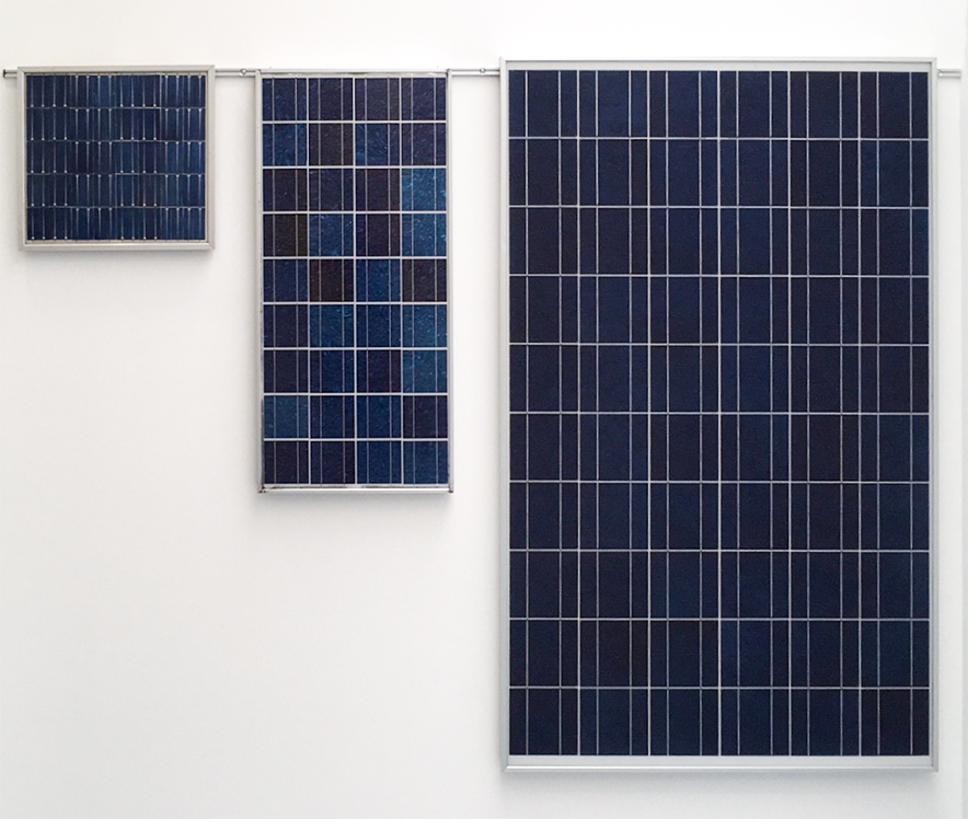 When you talk to the pioneers of the German PV industry, such as Mr. Udo Möhrstedt or the first participants of the symposium at Banz Monastery, one looks back at the early years with a sparkle in the eyes. A specific example is the comparison between the wafer sizes of the past and the present. The “wafer” is the starting material for the production of crystalline solar cells, which is only about 200 µm thick. Although there have been many adjustments over the years, the continuity has unfortunately disappeared. In recent months, countless new wafer sizes have appeared on the market. Something the PV industry has never experienced before. In addition, there is no uniform designation. With this article we would like to shed some light on the topic, and in addition to a review of the history of cell size, we want to compare the current common names. (more…)